
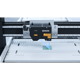
Semiconductor inspection sensor | Shape, thickness, and position measurement
For measuring the flatness and thickness of wafers, the coplanarity of BGAs, and the transport position. Here are examples from the semiconductor process.
We introduce measurement and inspection applications in semiconductor processes using SinceVision's 3D laser profilers, laser displacement sensors, spectral confocal displacement sensors, and transmission edge measurement sensors. Applications include measuring package flatness and parallelism, BGA solder ball coplanarity, wafer warpage, thickness, edge position, displacement of transport robots, and height measurement during dispensing. Depending on the measurement target and process, we select different sensor types and models. Please utilize this information to address on-site challenges such as shape acquisition of highly reflective surfaces and height measurement in limited installation spaces. If you provide us with the measurement target, required accuracy, takt time, and installation conditions, we can discuss configurations tailored to your applications.
- Company:SinceVision SinceVision
- Price:Other
